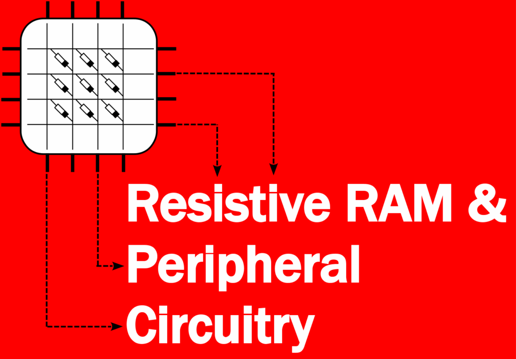
Link to Campo:
https://www.campo.fau.de:443/qisserver/pages/startFlow.xhtml?_flowId=detailView-flow&unitId=121793&periodId=565&navigationPosition=hisinoneLehrorganisation,examEventOverviewOwn
Lecturer: Dr.John Reuben Prabahar
Summary
Flash memory has been the de-facto standard for NVM (Non-Volatile Memories) for the last two decades and has been used in our computers, USB sticks, mobile phones and almost all electronic devices which need to retain some data without being powered ON. Due to technical limitations faced by flash memory, academia and industry have been researching new NVMs as replacement. Resistive Random Access Memory is one such promising NVM among other emerging Non-Volatile Memories (NVM). This course is aimed as an introductory course on ReRAM and In-Memory computing. First, the students will be introduced to this memory device and its characteristics. Then, memory array design is introduced. The peripheral circuitry i.e. the CMOS circuits around the memory for reading and writing into the memory array are elaborated. After the students become familiarized with the memory technology, they will be introduced to in-memory computing and how certain computing tasks can be implemented in the ReRAM array. In the accompanying exercises, the students will be taught how to simulate the memory array (using a ReRAM device model) and design the peripheral circuits using a transistor-level circuit-simulation tool (Cadence Virtuoso).
Note:
1. Students who register for this course must also register for the execise component „ReRAM and In-Memory Computing Exercise“ which is 2.5 ECTS.
2. It is NOT possible to register for the lecture component alone (2.5 ECTS) or exercise component alone (2.5 ECTS). Both must be registered (5 ECTS together) since the exercises closely follow the lecture.
Contents:
1. Concept of memory hierarchy, Advantages, evolution of memory hierarchy to include Storage class memory
(SCM).
2. SRAM, the standard for cache memory (Single bit SRAM Cell, READ/WRITE/HOLD operations)
3. DRAM, the standard for main memory (Single bit DRAM Cell, READ/WRITE/REFRESH operations)
4. Floating gate transistor (flash), the present standard for tertiary memory (cell structure, Array, READ/WRITE)
5. ReRAM as the emerging NVM, ReRAM Device Switching Charactersitics, Endurance, Retention,
charactersitics
6. Variability and Modeling of ReRAM
7. Resistive RAM Array Configurations (1R, 1S-1R, 1T-1R), Selectors for 1S–1R Array
8. Row Decoder, Column Multiplexer for Memory array
9. Three Ways to Increase Memory Density (Scaling, Multi level Cell, 3D stacking) Writing Multiple states and Reading multiple states
10. Voltage Mode Sensing, Time-based Sensing
11. Current-mode Sensing, ReRAM technology-specific issues to be considered while sensing ReRAM
12. Basic WRITE circuit and Voltage Regulation during WRITE operation,Incremental Program and Verify Approach
13. WRITE Termination Approach, Writing into 1S-1R arrays, Issues faced while writing into ReRAM cell
14. Von Neumann Bottleneck (The Memory Wall), In-memory Arithmetic (NOR and MAJORITY gate)
15. In-Memory Adders
16. Matrix Vector Multiplication(MVM) in ReRAM Array
17. Improved MVM using bit slicing
Recommended Requirements:
Students are recommended to have a basic knowledge of CMOS
(Complementary Metal Oxide Semiconductor) transistors, analog electronics
(differential amplifiers) and digital electronics (Flip-flops, Boolean logic gates).
This is usually acquired through a basic course on Integrated circuits/ Electronic
circuit design/ VLSI in the Bachelors/undergraduate level in most universities.
List degree programmes for which the module is intended:
– M.Sc. Information and Communication Technology
– M. Sc. Elektrotechnik, Elektronik und Informationstechnik
– M. Sc. Informatik
-M. Sc. Computational Engineering

