• Navigation überspringen
  • Zur Navigation
  • Zum Seitenende
Organisationsmenü öffnen Organisationsmenü schließen
Chair of Computer Science 3 (Computer Architecture)
  • FAUZur zentralen FAU Website
  1. Friedrich-Alexander-Universität
  2. Technische Fakultät
  • Lectures / Vorlesungen
  • Thesis / Abschlussarbeiten
  1. Friedrich-Alexander-Universität
  2. Technische Fakultät

Chair of Computer Science 3 (Computer Architecture)

Menu Menu schließen
  • Research
  • Teaching
  • Staff
  • Jobs
  1. Startseite
  2. Research
  3. Memristive Computing
  4. Experimental Setups

Experimental Setups

Bereichsnavigation: Research
  • AIMS
  • ECAS
  • Embedded Computing
  • ETI Projects
  • ETI: Energy-efficient Architectures
  • Former Projects
  • FORMUS³IC
  • HSA
  • IMBRA
    • Introduction
  • IntelRadar
  • KI-Flex
  • KI-Lernlabor
  • LO³-ML
  • LODRIC
  • Memristive Computing
    • History and Physical Properties
    • Multilevel Storage and Redundant Arithmetic
    • Experimental Setups
    • Simulation
  • MIMEC
  • Neuromorphic Computing
  • Non-Volatile Processors (NVPs)
  • Performance Modelling
    • Analytic modeling
    • Simulation
  • POV.OS
  • PowerSOC
  • ReLoFeMris
  • RISC-V
  • SDI
  • Smart PMU

Experimental Setups

MathJax.Hub.Config({tex2jax: {inlineMath: [[‚$`‘,’`$‘], [‚\\(`‘,’`\\)‘]]}});

div.wp-caption img{padding: .5em;}

Figure 1: Hardware Setup of Prototyping Platform
At PATMOS 2017 we presented our prototyping platform to the community1. You can see a picture of the hardware setup in Figure 1. Its purpose is to facilitate hardware design experiments with discrete, i.e. packaged, memristors. It is comprised of a FPGA (Figure 1a)) and an analog board (Figure 1b)). The analog board can drive memristors using 3-bit configurable pull-down resistor. An IP core for the FPGA is provided to facilitate setting and resetting by driving pulses, as well as reading out the Memristor. The read-out process is using a regulated (voltage follower) read voltage and a voltage divider. The signal of the voltage divider is then amplified and routed to the ADC of the FPGA. The circuitry can be seen in Figure 2.
Figure 2: Driving Circuitry

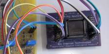
Since most researchers can not experiment with memristors embedded in their hardware, due to cost and technology issues, the memristors are attached as discrete devices (Figure 1c)). Using the setup we have implemented a small three-state register file and attached it to an implementation of the adder described in our article on redundant arithmetic.


  1. D. Wust, M. Biglari, J. Knödtel, M. Reichenbach, C. Söll and D. Fey, “Prototyping Memristors in Digital System with an FPGA-Based Testing Environment” International Workshop on Power And Timing Modeling, Optimization and Simulation (PATMOS) 2017, Thessaloniki, Greece, 2017, to be released in September↩
Friedrich-Alexander-Universität
Lehrstuhl für Informatik 3

Martensstrasse 3
91058 Erlangen
  • Impressum
  • Datenschutz
  • Barrierefreiheit
Nach oben