ASIC-Design
Complementary to our course „Einführung digitaler ASIC-Entwurf“, there is active research going on, when it comes to Hardware Design. The main focus points are Open Source tools for digital and mixed-signal design, high-level-synthesis for ASICS and Design-Space-Exploration for chiplets.
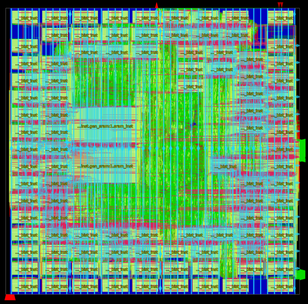
The image on the right side shows the layout of a fully connected layer within a convolutinal neural network we designed.
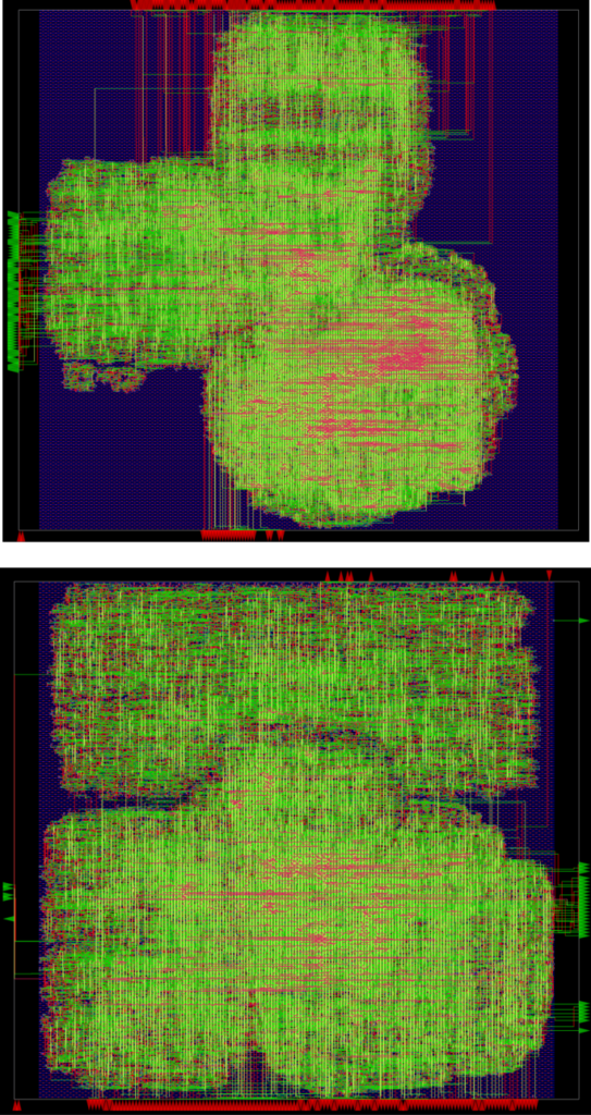
The layouts shown here illustrate the implementation at the layout level of two RISC-V processors. One is the NOVA architecture developed by Chair 3, which operates on operands represented internally in ternary form; the other, for comparison purposes, is the VexRISC-V architecture known from the literature.
The NOVA architecture uses a special ternary number representation for operands, known as the Canonical Signed Digit (CSD) representation.
In the signed digit representation, operands in individual digit positions can take not only 0 and 1, but also -1. This ternary redundant digit representation allows addition and subtraction to be performed independently of the word length N in two elementary steps, i.e., in O(1), whereas addition or subtraction with reasonable hardware complexity requires, at best, a complexity of O(log(N)), i.e., at least logN steps.
In the CSD digit representation, nearly half of all digits are guaranteed to be zero. This reduces the number of additions required in a multiplication by at least half, saving time and, in principle, energy. Analysis of the layouts generated using the design flow outlined below in the open-source design environment OpenLane revealed that the NOVA architecture achieves a 30% higher throughput, albeit at the cost of more area and power consumption. The latter is due to conversions between the CSD representation and two’s complement. However, there is still room for optimization in this area.
Details on the comparison of the two architectures can be found in the paper
Farhad EbrahimiAzandaryani, Michael Kupfer, Dietmar Fey: „Silicon-Based Evaluation of CSD Arithmetic in a RISC-V Processor Using Open-Source ASIC Flow“, to be published soon at IEEE International Symposium on Circuits and Systems (ISCAS) 2026 held in Shanghai.
RISC-V Design
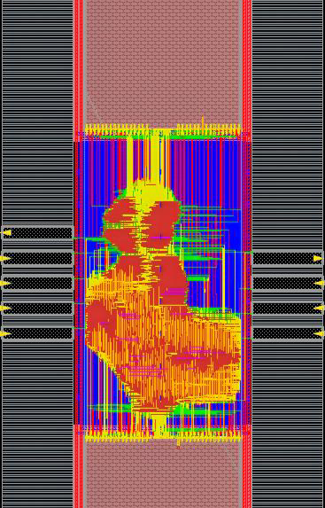
Neben der Nutzung von Open-Source-Entwicklungsumgebungen wurde mit den Cadence Entwicklungswerkzeugen eine weitere RISC-V-Architektur in Kooperation mit dem Leibniz-Institut für Mikroelektronik IHP in ein Layout übergeführt und zum Tape-Out gebracht. Es handelt sich um eine von der Universität Columbia offen gelegte und HL5 genannte spezifizierte RISC-V-Architektur, die High-Level-Synthese für RISC-V demonstriert. Diese wurde von uns in VHDL übertragen und an einer Stelle durch Forwarding optimiert.
Die Kooperation mit dem IHP geschieht im Rahmen des gemeinsamen DFG-Projektes „HYB-RISC“ im Rahmen des DFG-Schwerpunktprogrammes MEMRISTEC. Nach der Vermessung des realen Chips ist eine Erweiterung um hybride Register – bestehend aus RRAM und Flip-Flops – angestrebt. Diese hybriden Ansätze dienen der Energieoptimierung bei häufigen Leseoperationen, z.B. bei der Inferenz in Neuronalen Netzen.